Back drilling in PCB special process
What is back drilling
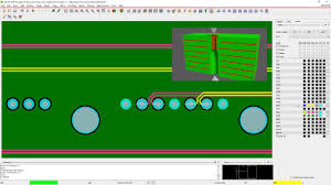
Back-drilling is a process of creating vias by removing short wires in a multilayer printed circuit board, facilitating the flow of signals from one layer of the board to another, ensuring that signals with the highest fidelity are transmitted at a faster speed.
For example, for 18-layer boards, we want them to be connected. In theory, we need to drill through holes and plate copper from layer 1 to layer 18. In fact, it is not necessary to go from the first to the 18th layer, as long as the through holes are in the first to the 16th layer. The 17th and 18th layers are not connected by wires, which affects the signal path and may cause signal integrity problems in the communication signal. We drilled the two layers from the back, which is called “STUB”, which reduces the difficulty and cost of the production process. The process first requires positioning holes for positioning and punching. Electroplate the first drilled PCB, seal the positioning hole with dry film before plating, make the outer layer pattern during the electroplating process, perform pattern plating on the PCB after the outer layer pattern is formed, and dry film seal the positioning hole before pattern plating. Then use the positioning hole used by the first drill bit for back drilling and positioning, and use the drill bit to back drill the electroplated holes that need to be back drilled. Finally, the drill bit needs to be cleaned, because the drill bit retains cuttings during back drilling.

Advantages of back drilling
1. Reduce noise interference.
2. Improve signal integrity.
3. Reduce the use of buried blind holes and reduce the difficulty of PCB manufacturing.
4. Compared with sequential lamination, the cost is lower.
5. Increase channel bandwidth
6. Data rate increase
7. Reduce the use of buried and blind holes, and reduce the difficulty of PCB production
Features of back drilling
* Most back drilling is rigid PCB
* Layers are generally 8 to 50 layers
* Thickness: 2.5mm or more
* PCB aspect ratio is large
* Large board size
* There are few traces on the outer layer, and most of them are designed with a square array of pressing holes
* Back-drilled through holes are usually 0.2mm larger than the through holes that need to be drilled
* Back drilling depth tolerance: +/- 0.05mm
* The minimum insulation thickness is 0.17mm
Difficulties of back drilling process
1. Back drilling depth control
Back drilling uses the depth control function of the drill bit to realize the processing of blind holes, and its tolerance is mainly affected by the accuracy of the back drilling equipment and the tolerance of the thickness of the medium. In addition, its accuracy is susceptible to external influences, such as the resistance of the drill bit, the angle of the drill bit, the contact effect between the cover plate and the measuring unit, and the warpage of the plate. Therefore, it is necessary to select suitable drilling materials and drilling methods in the production process to control the accuracy to achieve the best results.
2. Back drilling precision control
Back drilling is formed by secondary drilling according to the hole diameter of the primary drilling. The accuracy of the secondary drilling is very important. The expansion and contraction of the board, the accuracy of the equipment, and the way of punching will all affect the accuracy of the secondary punching, which is very important for the quality control of the PCB in the subsequent process.
Back drilling application
PCBs with back-drilling technology are mainly used in communication equipment, large servers, medical electronics, military, aerospace and other fields.

