What are PCB Plating Through Hole, Blind Via Hole and Buried Via Hole?
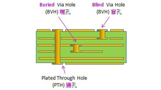
PCB vias are divided into three types: Plating Through Hole, Blind Via Hole and Buried Via Hole. The copper foil traces between conductive patterns in different layers of the circuit board are connected through vias.The printed circuit board is formed by the accumulation of many copper foil layers. The copper foil layers cannot communicate with each other because each layer of copper foil is covered with an insulating layer,so they need to rely on vias for signal connection.

Plating Through Hole
PlatingThrough holes are the most common and simplest type of guide holes. As long as the light is directed at the PCB, the hole that sees the bright light is the through hole. The production process is also very simple. We can just use a drilling tool to drill PCBs from top to bottom completely. The cost is relatively low, but it will take up more space. Although it is cheap, it is not very practical for every printed circuit board.
Blind Via Hole
Blind Via Hole refers to the electroplated holes which are connected the outermost circuit of the PCB to the adjacent inner layer. The opposite side cannot be seen, and the light cannot pass through, so it is called blind pass. In order to increase the space utilization of the PCB circuit layer, a blind via process was developed. This production method requires special attention to the depth of the drilling hole to be just right, otherwise it will often cause difficulties in electroplating in the hole, so most of pcb manufacturers have no capability to make blind vias. And the cost of blind via holes is more expensive than through holes. Thecircuit layer that needs to be connected can also be adjusted in advance In the case of individual circuit layers, holes are drilled first, and finally bonded together, but more precise positioning and alignment devices are required.
Buried Via Hole
Buried via hole means electroplated holes which are connected any internal circuit layers but not connected to the outer layer. This process cannot be achieved by drilling after lamination. It must be drilled at the timof individual circuit layers. After the inner layer is partially laminated, it must be electroplated before it can be fully laminated. Compared with the original plating through holes and blind via holes, buried hole process is more complicated, so the cost is the highest. This process is usually only used for high-density HDI circuit boards to increase the usable space of other circuit layers.
The use of Blind and Buried Via Holes
Usually used for complex PCB or HDI PCB, it can greatly reduce the size and quantity of PCB, reduce the number of layers, improve electromagnetic compatibility, increase the characteristics of electronic productsreduce costs, and also make the design work easier and faster. In traditional PCB design and processing, through holes will bring many problems. First, they occupy a lot of effective space, and secondly, a large numberof through holes are densely packed in one place, which also creates a huge obstacle to the wiring of the multilayer PCB. These plating through holes take up the space required for wiring, and they intensively passthrough the power supply and the ground. The surface of the wire layer will also destroy the impedance characteristics of the power ground wire layer and make the power ground wire layer ineffective.

PCB blind via holes and buried via holes need to be processed
1.Deep drilling method

2.Sequential lamination

3.HDI accumulation

Our manufacturing capabilities
1. Number of layers: up to 20 layers
2. Minimum aperture: laser drill 0.1mm, traditional drill 0.2mm
3. Aspect ratio: traditional drilling <12:1, laser drilling> 0.75:1

